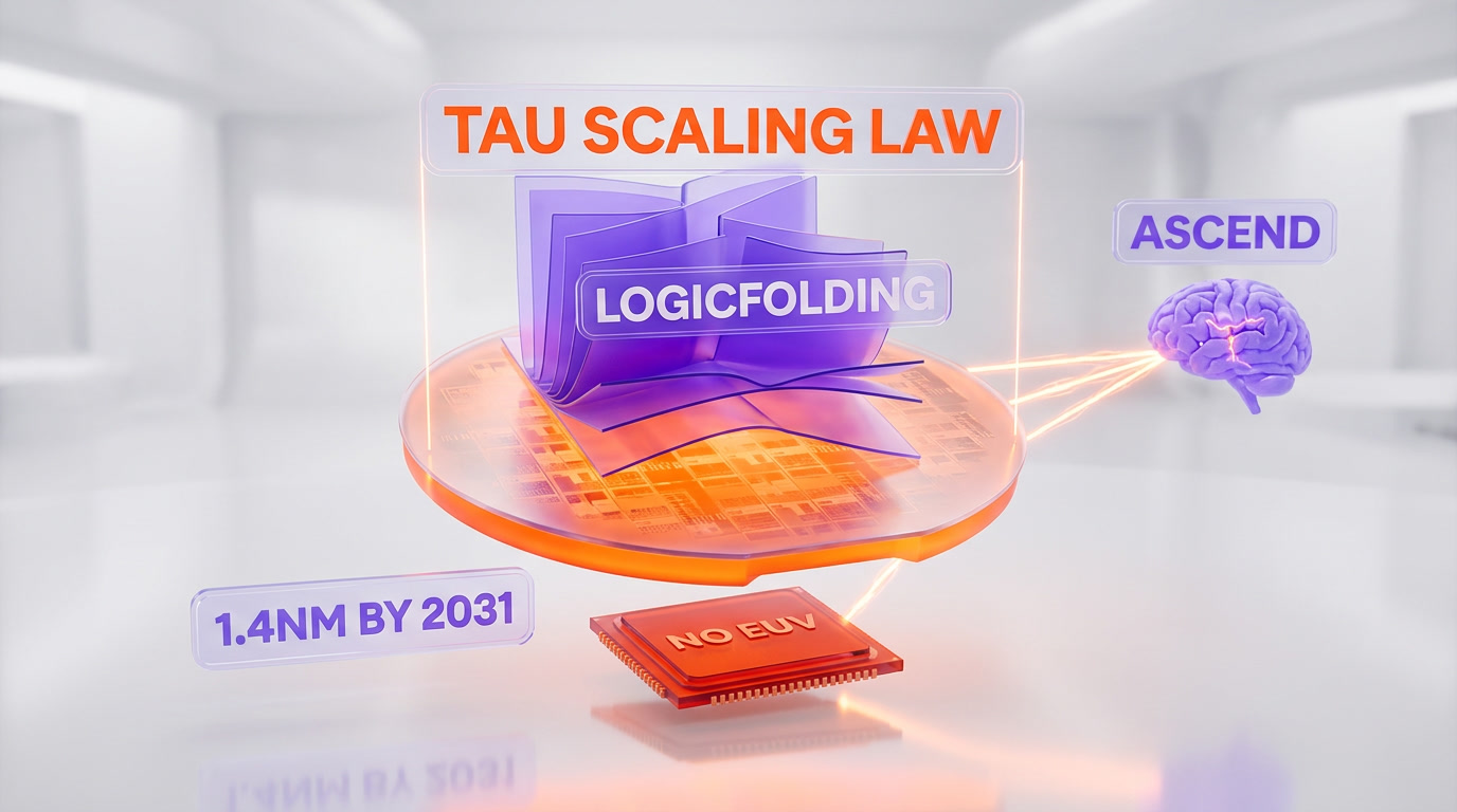
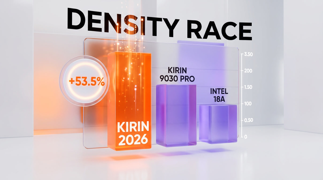
Huawei's Tau Scaling Law is a chip-design framework, unveiled May 25 2026 by Huawei semiconductor chief He Tingbo, that aims to keep improving performance by cutting signal and data transmission time rather than shrinking transistors. Paired with a vertical 3D stacking architecture called LogicFolding, Huawei says it can reach 1.4nm-equivalent transistor density by 2031 — roughly three years behind TSMC's projected timeline — entirely without ASML's EUV lithography, which China cannot legally buy. The first chips to use LogicFolding are the Kirin mobile processors launching in fall 2026, which TrendForce measures at 238 million transistors per square millimeter, up 53.5% from the Kirin 9030 Pro and theoretically comparable to Intel 18A.
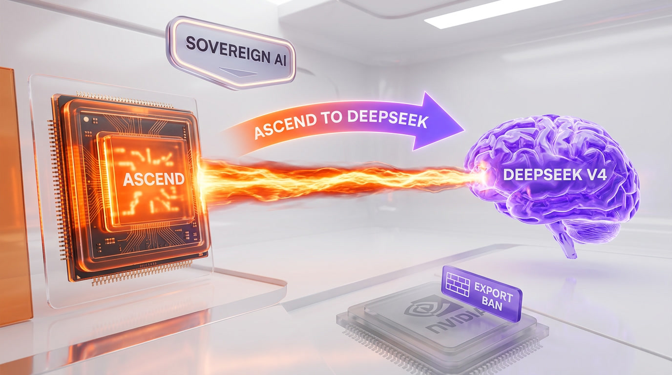
For an AI ecosystem, the headline is not the phone chip. It is what sits underneath the entire Chinese AI stack. Huawei's Ascend accelerators increasingly power Chinese frontier models — including DeepSeek V4 — and a denser, EUV-free manufacturing path is exactly the kind of supply-chain insurance that lets Chinese labs keep training and serving models even as US export controls tighten. The announcement, first reported by Bloomberg, reads as China narrowing the gap with TSMC and the Nvidia-led AI-hardware order, even if analysts agree the country still trails at the most advanced nodes.
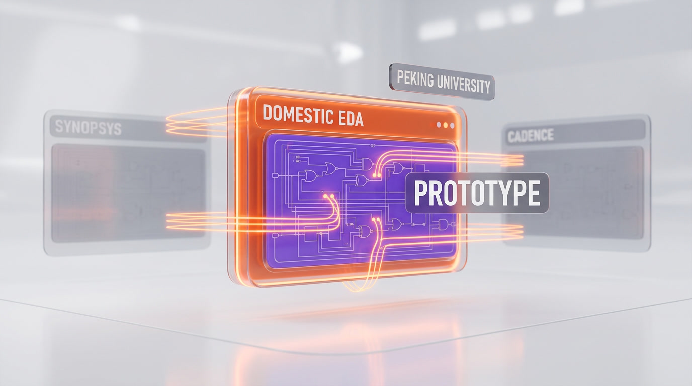
Two days later, on May 27 2026, the announcement got a software bookend. The School of Integrated Circuits at Peking University showed a prototype domestic EDA (electronic design automation) tool built to be compatible with LogicFolding — a research effort aimed at loosening China's dependence on Western leaders Synopsys and Cadence. It is a prototype, not a production toolchain, but it points at the same goal as the hardware work: an AI-chip pipeline that does not depend on tools Washington can switch off.
The AI Angle First: Sovereign Silicon Under the Models
Most coverage of this story frames it as a smartphone-chip race. We think that misses the point for anyone who cares about AI. The reason a Tau Scaling Law announcement matters to model builders is that compute is the binding constraint on Chinese AI, and Huawei is the company trying to relieve it from inside the country's borders.
Huawei's Ascend line — the 910-series accelerators and the CloudMatrix systems built around them — is the domestic answer to Nvidia's H100 and B200 GPUs that Chinese firms can no longer freely import. When DeepSeek shipped V4 in April 2026, the broader story was not only the model's hybrid-attention architecture and 1M-token context window; it was that an increasingly large share of Chinese training and inference is migrating onto Ascend silicon. We covered that launch in our breakdown of DeepSeek V4, and the through-line is the same: the model layer is moving as fast as the hardware layer underneath it allows.
That is why a manufacturing breakthrough — even a partial, slower-than-TSMC one — changes the calculus. If Huawei can keep pushing density and performance without EUV, the ceiling on how big and how cheap Chinese AI training runs can get rises with it. The Tau Scaling Law is, in effect, a bet that China can keep the AI flywheel spinning without the one machine it is forbidden from owning.
What Huawei Actually Announced
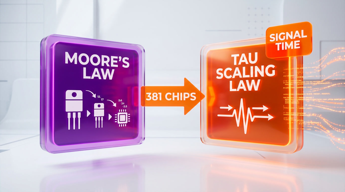
On May 25 2026, He Tingbo, the head of Huawei's semiconductor business, presented two linked ideas. The first is the Tau Scaling Law, positioned explicitly as an alternative to Moore's Law. Where Moore's Law tracks progress by how small you can make a transistor, the Tau approach reframes the objective: reduce the time it takes signals and data to move through and between chips. He Tingbo said Huawei has designed 381 chips over six years using this approach — a number meant to signal that this is an operating methodology, not a slideware concept.
The second is LogicFolding, a vertical 3D stacking architecture. Instead of laying logic out flat and relying on ever-finer lithography to pack more transistors into a 2D plane, LogicFolding folds logic upward into stacked layers. That shortens the physical distance signals travel, which is the whole point of the Tau framing — and it sidesteps the part of the race where you need EUV machines to keep shrinking 2D features.
Why "Without EUV" Is the Headline
Extreme ultraviolet (EUV) lithography is the chokepoint. ASML, the Dutch company, is the only supplier of EUV scanners, and under US-led export controls those machines cannot be sold to China. The conventional path to leading-edge nodes — 3nm, 2nm, and below — runs straight through EUV. Cut off from it, the obvious conclusion is that China simply cannot reach the frontier.
Tau Scaling Law plus LogicFolding is Huawei's argument that the conclusion is wrong, or at least not absolute. By optimizing signal time and stacking vertically rather than shrinking horizontally, Huawei claims it can reach transistor density equivalent to a 1.4nm node by 2031, against TSMC's projected timeline of roughly 2028 for comparable density. That is a gap measured in years, not generations — and it is a gap Huawei says it can close using deep ultraviolet (DUV) tools it already has, multi-patterning, and architecture rather than the EUV machines it does not.
It is worth being precise about the claim. Huawei is not saying it has matched TSMC today. It is saying it has a credible roadmap to a specific density target on a specific date without the tool everyone assumed was mandatory. Analysts remain skeptical that the most advanced nodes are reachable this way at scale, and yield and cost are open questions. But the framing has shifted from "China is locked out" to "China has a slower, different route in."
The Kirin 2026: First Silicon to Carry LogicFolding
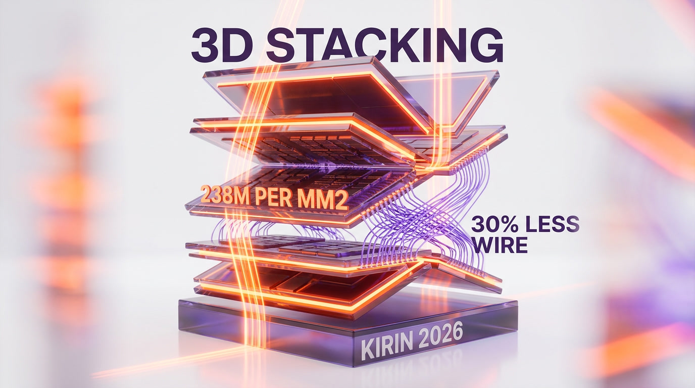
The proof point arrives this fall. Huawei's Kirin mobile chips launching in autumn 2026 will be the first commercial silicon built on LogicFolding. According to TrendForce, the Kirin 2026 reaches 238 million transistors per square millimeter — a 53.5% jump over the Kirin 9030 Pro and a figure the firm describes as theoretically comparable to Intel 18A and close to the first generation of TSMC's 3nm process.
That last comparison is the one that should make AI-hardware watchers sit up. If a Chinese-designed, non-EUV chip can land in the same density neighborhood as Intel 18A and early TSMC 3nm, the practical distance between "what China can build" and "what the leading foundries ship" is smaller than the export-control narrative implies. The Kirin is a phone chip, but the manufacturing learning — the stacking, the routing, the thermal management — transfers toward the data-center silicon that actually trains and serves AI models.
Density Is Not the Same as Node Leadership
We want to be honest about what 238 million transistors per square millimeter does and does not mean. Transistor density is one axis. Power efficiency, clock frequency, yield, and cost per good die are the others, and they are where leading-edge EUV nodes still pull ahead. A dense chip that runs hot, yields poorly, or costs too much to fabricate at volume is not a frontier chip. Huawei's claim is genuinely impressive on the density axis; the open questions live on the others. For AI workloads specifically — where performance per watt across thousands of accelerators decides total cost of training — efficiency may matter more than raw density.
The Software Half: A Domestic EDA Tool for LogicFolding
Hardware is only half of a chip pipeline. The other half is EDA — the electronic design automation software engineers use to lay out, route, and verify a chip before it is ever fabricated. This is a market dominated by three Western firms, with Synopsys and Cadence at the top. For all the attention on EUV machines, EDA software is an equally hard dependency to replace, and it is just as exposed to export restrictions.
On May 27 2026, the School of Integrated Circuits at Peking University unveiled a prototype domestic EDA tool designed to be compatible with LogicFolding. The explicit goal is to reduce China's reliance on Synopsys and Cadence. We want to flag clearly: this is a research prototype, not a production-ready toolchain. It is not going to replace commercial EDA suites this year, and the gap between a working demo on open-source designs and a hardened tool that chip companies trust with billion-transistor products is enormous.
What is interesting is the early result. Peking University's team reported that applying their 3D-aware EDA approach to open-source designs cut total intra-chip wire length by roughly 30% compared with conventional 2D design software. Shorter wires mean faster signals, lower power, and better heat distribution — which is exactly what the Tau Scaling Law is optimizing for. In other words, the software and the architecture are pointed at the same target: get more out of the chip by moving data less distance, instead of by shrinking features the country cannot shrink.
Why a 30% Wire-Length Cut Matters for AI Chips
It is easy to read "30% shorter wires" as a niche engineering metric. For AI accelerators it is not. In modern AI chips, a large and growing share of energy is spent not on computation but on moving data — between memory and logic, and across the chip's own fabric. The further data has to travel, the more power it burns and the more heat it generates, which in turn caps how densely you can pack accelerators in a data center.
If a 3D-aware design flow can structurally cut interconnect length, it attacks the exact bottleneck that limits AI training efficiency at scale. This is conceptually adjacent to a broader industry push to wring more performance out of every watt rather than every nanometer. We have written about one of the more radical versions of that idea in our piece on MIT's waste-heat analog computing, and while the technologies are completely different, the strategic logic rhymes: when you cannot win the raw-node race, you win on architecture and efficiency.
How This Fits the Broader Chip-Decoupling Story
None of this is happening in a vacuum. The Tau Scaling Law announcement lands in the middle of a multi-year decoupling between the US and Chinese semiconductor ecosystems — a separation that now runs in both directions. The US restricts the export of EUV machines, leading-edge GPUs, and increasingly the EDA software and design IP that underpin them. China, in turn, has built parallel supply chains and tightened its own controls.
That tit-for-tat now extends to people, not just machines. We looked at the human-capital side in our analysis of China's AI talent travel curbs, which mirror US chip controls by restricting the outbound flow of expertise the same way Washington restricts the outbound flow of hardware. Huawei's announcement is the manufacturing-side complement: if you cannot import the frontier, you build a domestic path toward it, and you build the talent and tooling to walk that path.
The capital side of the story is moving too — and not only inside China. Western players are racing to lock up alternative AI-silicon architectures, as we covered in our report on Fractile's $220M Series B and Anthropic's UK silicon shopping. The common thread across all of these stories is that the AI-hardware layer has become the contested ground. Models are downstream of chips, chips are downstream of tools and fabs, and every major player — Huawei, Nvidia, TSMC, ASML, the labs, and the governments behind them — is now maneuvering at the hardware layer because that is where the leverage lives.
What This Means for Nvidia and TSMC
For Nvidia, the immediate effect is limited and the long-term effect is real. Nvidia's data-center GPUs remain the global standard, and even Chinese labs would still prefer them where they can get them. But every credible step Huawei takes toward viable domestic accelerators erodes the assumption that Chinese AI is structurally throttled by hardware. If Ascend keeps improving and the manufacturing path keeps widening, the addressable market Nvidia loses to export controls becomes a market it loses to a competitor instead.
For TSMC, the framing is different. TSMC is not just a chipmaker; it is the foundry the entire fabless world depends on, including Nvidia, Apple, and AMD. A Chinese path to dense silicon without EUV does not threaten TSMC's customers tomorrow. But it does chip away at the strategic premise that leading-edge manufacturing is a moat only TSMC and a couple of others can ever cross. The Tau Scaling Law is, in part, an argument that the moat has more than one bridge — even if the alternative bridge is slower and narrower.
The Skeptic's Case
We do not want to oversell this. There are good reasons to treat Huawei's claims with caution. Announcements like this serve a strategic and political purpose, and a 2031 density target is far enough out that it cannot be verified now. Density equivalence does not equal node equivalence; yield, cost, and power efficiency remain the hard parts, and they are precisely the parts EUV nodes are best at. The Peking University EDA tool is a prototype on open-source designs, not a battle-tested suite that ships commercial AI chips. And independent analysts continue to say China trails at the most advanced nodes — which Huawei itself implicitly concedes with a multi-year timeline.
The honest read is somewhere between the hype and the dismissal. China is not at the frontier. But the gap is being framed in years rather than as a permanent lockout, the manufacturing approach is genuinely different rather than a copy of the EUV path, and the AI-relevant metric — efficiency through shorter data paths — is exactly the one that matters most for training and serving large models at scale.
Our Take
We have been tracking the AI-hardware decoupling closely, and the Tau Scaling Law plus LogicFolding is one of the more substantive moves we have seen from the Chinese side this year. It is not a "China caught up" story. It is a "China found a different door" story, and the door it found — optimizing for signal time and data movement rather than feature size — happens to be aligned with where AI-chip efficiency is heading anyway.
The piece we will be watching is the translation from phone silicon to data-center silicon. The Kirin 2026 proves the manufacturing approach works at the consumer scale. The real question for the AI world is whether the same stacking, routing, and thermal techniques carry over to the Ascend accelerators that train models like DeepSeek V4 — and whether the domestic EDA effort matures fast enough to design those chips without Synopsys and Cadence. If both happen, the export-control thesis weakens considerably. If neither does, this stays an impressive but contained achievement.
What's Next
The near-term milestone is the fall 2026 Kirin launch, which will let independent labs measure LogicFolding silicon directly rather than relying on TrendForce projections. After that, the signals to watch are whether Huawei applies the architecture to a next-generation Ascend accelerator, whether the Peking University EDA prototype moves from open-source demos toward real chip tape-outs, and whether the claimed 1.4nm-equivalent density roadmap holds its 2031 date as fabrication realities set in. Each of those would mark another step in China building an AI-chip pipeline that does not run through ASML, Synopsys, Cadence, or TSMC — and each would reshape how the global AI-hardware map looks by the end of the decade.
Frequently Asked Questions
What is Huawei's Tau Scaling Law?
The Tau Scaling Law is a chip-design framework Huawei unveiled on May 25 2026, positioned as an alternative to Moore's Law. Instead of tracking progress by shrinking transistors, it focuses on reducing the time signals and data take to move through and between chips. Huawei semiconductor chief He Tingbo said the company has designed 381 chips over six years using this approach.
What is LogicFolding?
LogicFolding is Huawei's vertical 3D stacking architecture, announced alongside the Tau Scaling Law. Rather than laying logic out flat and relying on finer lithography, it folds logic upward into stacked layers to shorten the physical distance signals travel. The Kirin mobile chips launching in fall 2026 will be the first commercial silicon to use it.
Can Huawei really match TSMC without EUV lithography?
Huawei claims it can reach transistor density equivalent to a 1.4nm node by 2031 without ASML's EUV machines, against TSMC's projected timeline of roughly 2028 for comparable density. That is a gap of about three years, not a permanent lockout. However, analysts caution that density equivalence is not node equivalence — yield, cost, and power efficiency are where leading-edge EUV nodes still pull ahead.
Why can't China buy EUV machines?
ASML, the Dutch company, is the only supplier of EUV lithography scanners, and under US-led export controls those machines cannot be sold to China. EUV is the conventional path to leading-edge 3nm and 2nm nodes, so being cut off from it is the central reason China was assumed to be locked out of frontier chips. Huawei's Tau Scaling Law and LogicFolding are its argument for a different route.
How dense is the Kirin 2026 chip?
According to TrendForce, the Kirin 2026 reaches 238 million transistors per square millimeter — a 53.5% increase over the Kirin 9030 Pro. TrendForce describes that figure as theoretically comparable to Intel 18A and close to the first generation of TSMC's 3nm process. It will be the first chip built on the LogicFolding architecture.
How does this connect to Chinese AI models like DeepSeek?
Huawei's Ascend accelerators increasingly power Chinese frontier AI models, including DeepSeek V4. A denser, EUV-free manufacturing path gives Chinese AI labs supply-chain insurance to keep training and serving models despite US export controls on Nvidia GPUs. The chip story is, underneath, a story about whether China can keep scaling sovereign AI compute.
What is the Peking University EDA tool?
On May 27 2026, the School of Integrated Circuits at Peking University unveiled a prototype domestic EDA (electronic design automation) tool built to be compatible with LogicFolding. The goal is to reduce China's reliance on Western leaders Synopsys and Cadence. It is a research prototype, not a production-ready toolchain.
What did the early 3D EDA tests achieve?
Peking University reported that applying its 3D-aware EDA approach to open-source designs cut total intra-chip wire length by roughly 30% compared with conventional 2D design software. Shorter wires mean faster signals, lower power, and better heat distribution — the same goals the Tau Scaling Law is optimizing for.
Why does a 30% wire-length reduction matter for AI accelerators?
In modern AI chips, a large share of energy is spent moving data rather than computing it. The further data travels, the more power it burns and heat it generates, which caps how densely accelerators can be packed in a data center. Structurally cutting interconnect length attacks the exact bottleneck that limits AI training efficiency at scale, which is why this metric matters more for AI than raw transistor density.
What does this mean for Nvidia and TSMC?
For Nvidia, every credible step toward viable Chinese accelerators erodes the assumption that Chinese AI is structurally throttled by hardware, turning a market lost to export controls into a market lost to a competitor. For TSMC, a Chinese path to dense silicon without EUV does not threaten its customers tomorrow, but it weakens the premise that leading-edge manufacturing is a moat only a couple of foundries can ever cross.
Is China now caught up with TSMC and the West in chips?
No. Independent analysts agree China still trails at the most advanced nodes, and Huawei's own multi-year timeline implicitly concedes this. The shift is in framing — from "China is locked out" to "China has a slower, different route in." Density equivalence claims do not equal full node equivalence on yield, cost, and power efficiency.
When can these claims be independently verified?
The near-term milestone is the fall 2026 Kirin launch, which will let independent labs measure LogicFolding silicon directly rather than relying on TrendForce projections. Longer-term signals include whether Huawei applies the architecture to a next-generation Ascend accelerator, whether the Peking University EDA prototype reaches real chip tape-outs, and whether the 1.4nm-equivalent density roadmap holds its 2031 date.