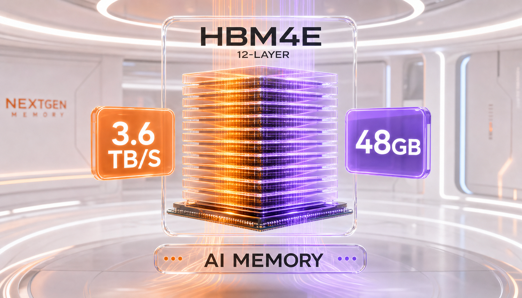
Samsung's 12-layer HBM4E is the industry's first sample of next-generation High Bandwidth Memory, the stacked DRAM that feeds data to AI accelerators. Announced on May 29, 2026, each 12-high stack delivers 3.6 terabytes per second of bandwidth — more than 20% above HBM4 — and 48 GB of capacity, roughly 30% more than the previous generation. By shipping samples first, Samsung moves roughly six months ahead of SK Hynix and retakes the technical lead in AI memory.
What Happened
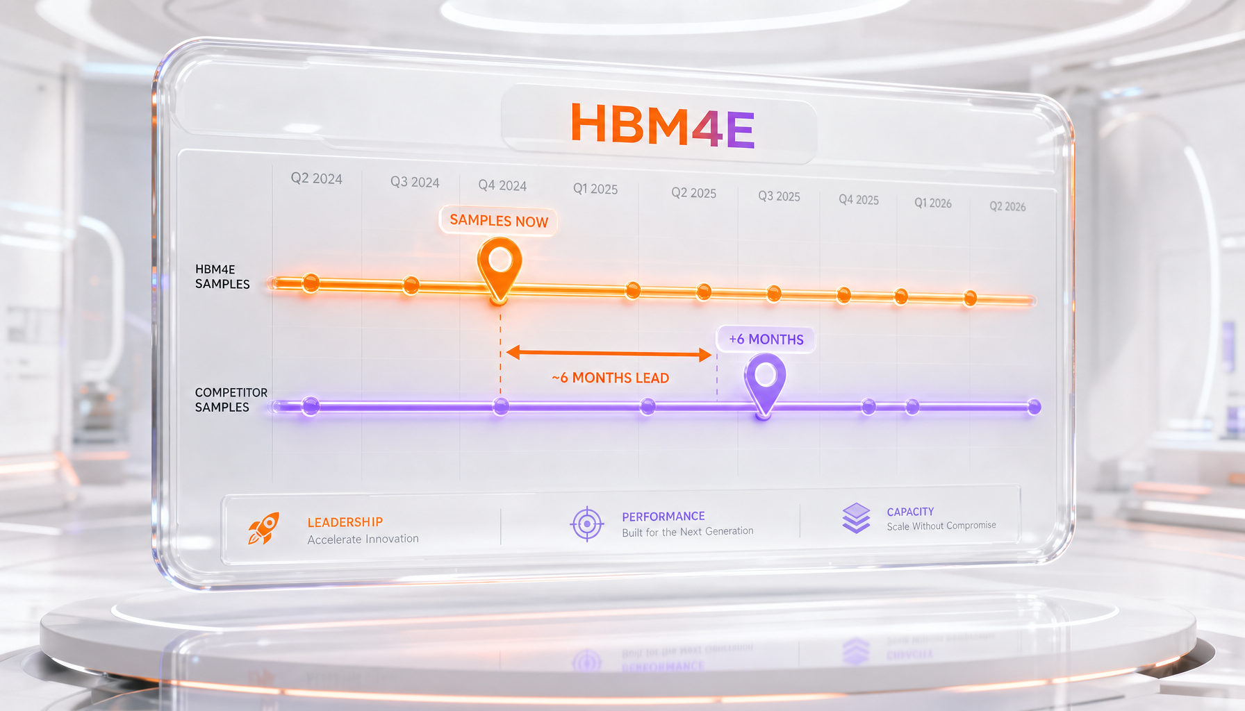
Samsung said this week that it has begun shipping the industry's first 12-layer HBM4E memory samples to major customers. The announcement, dated May 29, 2026, with follow-on reporting on May 30, marks the opening move in the next chapter of the High Bandwidth Memory race — the slice of the DRAM market that has quietly become one of the most strategically important in all of computing.
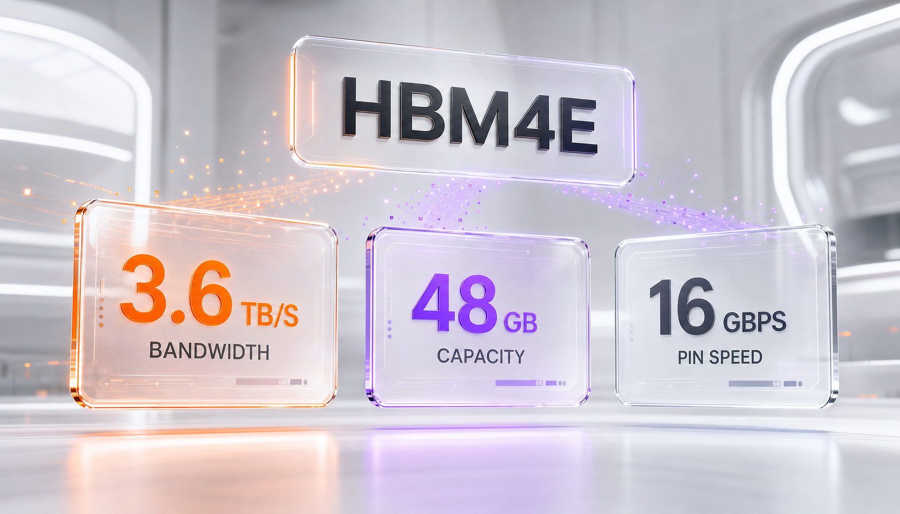
The headline specifications are aggressive. Each 12-high HBM4E stack delivers 3.6 terabytes per second of bandwidth per stack, which Samsung pegs at more than 20% above HBM4. Capacity climbs to 48 GB per stack, about 30% more than the previous generation. Pin speeds sit around 14 Gbps and scale up to 16 Gbps. Those are not incremental gains; they are the kind of step that determines whether the next generation of AI accelerators is fed fast enough to keep their compute cores busy.
Sang Joon Hwang, Executive Vice President and Head of Memory Development at Samsung, framed the milestone in competitive terms: "Following the successful mass production of HBM4, Samsung has once again demonstrated its distinct technological edge with HBM4E." The subtext is hard to miss — Samsung wants the market to read HBM4E as proof that it has closed the gap with SK Hynix, the company that has dominated HBM for the better part of a decade.
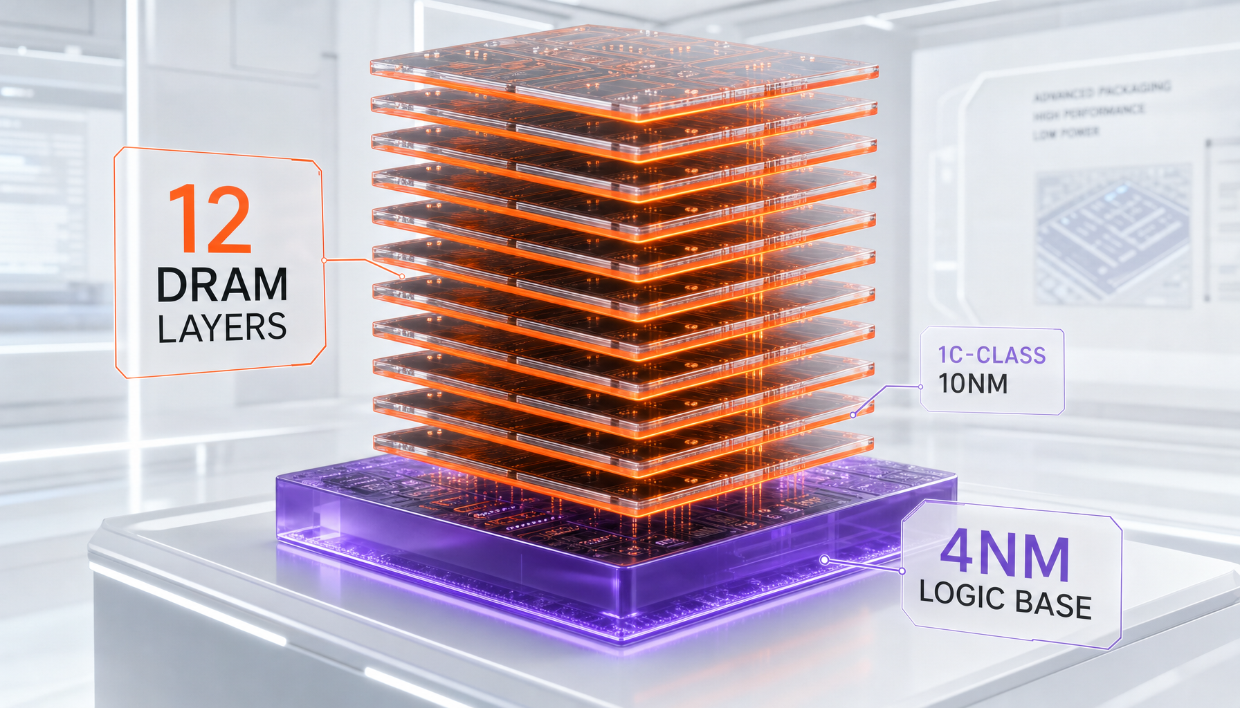
On the manufacturing side, Samsung built the 12-layer HBM4E on its 1c-class 10nm DRAM process for the memory dies, paired with a logic base die fabricated on its own 4nm foundry process. That combination of a leading-edge DRAM node and an in-house 4nm logic base die is a vertical-integration play few rivals can match cleanly, and it sits at the heart of why this sample matters beyond the raw numbers.
The Numbers That Matter
To understand why a memory sample is making headlines, it helps to be precise about what HBM4E actually delivers. Here is the spec sheet in plain terms.
| Metric | Samsung 12-layer HBM4E | Versus prior generation |
|---|---|---|
| Bandwidth per stack | 3.6 terabytes per second | More than 20% above HBM4 |
| Capacity per stack | 48 GB (12-high) | About 30% more |
| Pin speed | ~14 Gbps, scaling to 16 Gbps | Higher signaling rate |
| DRAM process | 1c-class 10nm | Leading-edge node |
| Logic base die | In-house 4nm foundry | Vertical integration |
The single most important figure is bandwidth. At 3.6 terabytes per second per stack, HBM4E can move data to and from an AI accelerator faster than almost anything else on the market. For large language models, memory bandwidth — not raw compute — is frequently the true bottleneck. A model spends a surprising amount of its time waiting for weights and activations to arrive from memory. Lift the bandwidth ceiling by more than 20%, and you lift the practical ceiling on training throughput and inference latency at the same time.
Capacity is the second lever. At 48 GB per stack, a handful of HBM4E stacks around a single accelerator can hold a far larger slice of a model close to the compute cores. That reduces the need to shuffle data across slower interfaces, which is exactly the kind of friction that drags down efficiency in modern AI clusters. We have covered how the broader industry is attacking the same problem from other angles — from MIT's waste-heat analog computing experiments to entirely new inference-chip architectures from startups like Fractile — and faster, denser memory is one of the most direct paths to squeezing more out of every watt.
Why It Matters
High Bandwidth Memory is the unsung half of the AI hardware story. When people talk about AI accelerators, they almost always mean the compute die — the GPU or custom ASIC. But every one of those chips is ringed by HBM stacks, and the performance of the whole package is gated by how fast and how much memory sits beside the compute. You can build the fastest matrix-multiply engine in the world, and it will still stall if it cannot be fed.
That is why a 12-layer HBM4E sample is genuinely consequential rather than a footnote. The memory makers — Samsung, SK Hynix, and Micron — are effectively a supply-chain chokepoint for the entire AI buildout. The accelerator designers depend on them, and the timing of HBM availability can shape product roadmaps a year or more in advance. When Samsung ships the first HBM4E samples, it is signaling to NVIDIA, AMD, and the hyperscalers that it can be a primary supplier for the next hardware generation.
There is also a strategic narrative here. SK Hynix has been the HBM leader, riding that advantage into outsized profits as demand exploded. Samsung spent the HBM3 and early HBM4 era playing catch-up on qualification timelines. HBM4E is the moment Samsung is choosing to reassert itself. Shipping the industry's first 12-layer samples is not just a spec win; it is a positioning statement aimed squarely at the company that has been eating its lunch in AI memory.
The same supply-chain logic is why so much capital and engineering attention is flowing into the layer beneath the models. The companies designing the chips know that memory, packaging, and power are now the constraints that matter. We have written about how even model labs like Mistral are exploring custom silicon and how power availability has become its own bottleneck. HBM4E slots directly into that picture: better memory makes every other dollar spent on accelerators and data centers go further.
How HBM4E Is Built
The architecture is worth unpacking because it explains Samsung's edge. An HBM4E stack is not a single chip. It is a tower of DRAM dies — twelve of them in the 12-high configuration — bonded vertically and connected to a logic base die at the bottom. The base die acts as the controller and interface, marshaling data in and out of the stack and talking to the accelerator through a wide, dense set of connections.
Samsung fabricated the DRAM dies on its 1c-class 10nm process, the leading edge of its memory technology. The logic base die, however, came from Samsung's own 4nm foundry process. That detail is the strategic core of the announcement. Most memory makers have to source advanced logic from an outside foundry. Samsung can build both the memory and the logic base die in-house, which lets it co-optimize the two layers and control its own supply chain from end to end.
Stacking twelve dies and keeping the whole package thermally and electrically sound is a brutal engineering challenge. Each additional layer adds height, heat, and signal-integrity risk. Hitting 3.6 terabytes per second across a 12-high stack while keeping pin speeds in the 14 to 16 Gbps range is a demonstration of advanced packaging and thermal design as much as it is a memory milestone. This is precisely the kind of 3D-stacking and packaging expertise that the whole industry is racing to master — China's chipmakers are pursuing their own version of the same idea, as we covered in our look at Huawei's 3D LogicFolding architecture.
How It Compares: The Three-Way HBM Race
The HBM market has effectively three suppliers, and HBM4E throws their relative positions into sharp relief.
SK Hynix has been the incumbent leader, the default HBM supplier for the highest-end AI accelerators through the HBM3 and HBM3E era. On HBM4E, though, SK Hynix is reportedly targeting samples in the second half of 2026 and mass production in 2027. That puts Samsung roughly six months ahead on the sample timeline — a meaningful gap in a market where qualification windows decide which supplier wins the design slot for a given accelerator generation.
Samsung, with this announcement, is the first to ship 12-layer HBM4E samples. If it can convert that sample lead into qualified, high-yield mass production, it stands to capture share at exactly the moment demand for next-generation AI memory is peaking. The in-house 4nm logic base die is its differentiator.
Micron, the third major supplier, has not announced HBM4E as of this news. Micron has been a credible HBM3E player and a key second source for some customers, but on HBM4E specifically it has stayed quiet, leaving the early HBM4E narrative to Samsung and SK Hynix.
The takeaway is that Samsung has, at least for now, the clearest claim to the HBM4E lead. Sampling first does not guarantee winning the contracts — yield, reliability, and price still decide who gets designed into NVIDIA's and AMD's next accelerators — but being first to sample is a strong opening position, and it resets the competitive story that SK Hynix had been controlling.
Who This Affects
The most obvious beneficiaries are the accelerator designers. NVIDIA and AMD are reportedly among the customers these samples are aimed at, along with major hyperscalers building their own AI silicon. Their next-generation GPUs and accelerators need exactly what HBM4E offers: more bandwidth to keep ever-larger compute dies fed, and more capacity to hold bigger models on-package. We have tracked how central this hardware layer has become to the entire AI economy, from NVIDIA's Vera Rubin roadmap and its trillion-dollar order book to the independent benchmarks of its Vera CPU. Every one of those accelerators is gated by the memory beside it.
Hyperscalers and AI labs are the second-order beneficiaries. Faster HBM means more efficient training and inference, which means lower cost per token and the ability to serve larger models at acceptable latency. In a year where the economics of running frontier models are under intense scrutiny, anything that improves the bandwidth-per-dollar and capacity-per-dollar math matters.
And then there is the competitive dynamic among the memory makers themselves. SK Hynix has enjoyed premium pricing and priority allocation as the HBM leader. A credible Samsung challenge on HBM4E could shift bargaining power, introduce more supply competition, and ultimately give accelerator buyers a stronger second source. For an industry that has worried constantly about HBM being a single-vendor chokepoint, a genuine two-horse race at the leading edge is healthy.
The Caveats
It is worth being disciplined about what a sample shipment is and is not. Sampling means Samsung has working 12-layer HBM4E parts good enough to put in customers' hands for evaluation. It does not mean those parts are qualified at volume, that yields are economical, or that any specific customer has committed to buying them. The history of HBM is full of suppliers who sampled early and then stumbled on yield or reliability at scale.
Samsung has also not published a firm mass-production date for HBM4E in this announcement, and it has not officially named a single customer. The NVIDIA, AMD, and hyperscaler targets are reported rather than confirmed by Samsung. We are treating those attributions as reporting, not as official commitments, and the prudent reader should too.
The competitive timeline could also compress. SK Hynix targeting second-half 2026 samples means Samsung's roughly six-month lead is a snapshot, not a moat. If SK Hynix executes well and Samsung hits yield trouble, the order of the race could change quickly. HBM is a market where a single qualification slip can cost a supplier a whole product generation's worth of design wins.
The Bigger Supply-Chain Picture
Step back from the spec sheet and HBM4E fits into a story the industry has been telling itself with growing urgency: AI's limiting factor is no longer the model architecture or even the headline compute number on an accelerator. It is the surrounding system — memory, advanced packaging, interconnect, and power. Each of those has become its own competitive battleground, and HBM sits at the intersection of the first two.
Consider the dependency chain. An AI lab wants to train or serve a larger model. To do that economically, it needs accelerators with more usable memory bandwidth and capacity. Those accelerators need HBM stacks that can deliver it. The HBM stacks need both leading-edge DRAM and advanced packaging to bond a dozen dies together without cooking them. And the whole assembly needs enough power and cooling to run at scale. Samsung's HBM4E announcement is one link in that chain getting stronger — but it only pays off if the links around it keep pace.
This is also why the financial stakes around HBM have become so large. The suppliers who lead at the leading edge command premium pricing and priority allocation, and the buyers — NVIDIA, AMD, and the hyperscalers — plan their roadmaps around who can deliver. A shift in HBM leadership is not a niche memory-industry story; it ripples through the capital expenditure plans of the largest technology companies on earth. When Samsung says it has the industry's first 12-layer HBM4E, it is making a claim on a slice of that spending.
For builders and operators watching from outside the memory industry, the practical signal is simpler. The next generation of AI hardware is going to be meaningfully more capable on the memory axis, and it is arriving on a sample-to-production timeline that points toward broad availability in the 2026 to 2027 window. If your roadmap depends on bigger models running at lower cost, the memory side of the equation is finally moving in your favor — and a real two-supplier race at the leading edge is the best guarantee that those gains keep coming.
Our Take
We read this as the most important signal yet that Samsung intends to win back the AI memory crown rather than settle for second source. The specs are real and they are aggressive: 3.6 terabytes per second of bandwidth and 48 GB of capacity per stack are the kind of numbers that change what the next generation of accelerators can do. But the part we find most telling is the in-house 4nm logic base die. That is Samsung leaning on a structural advantage — owning both the memory and the foundry — that SK Hynix and Micron cannot easily replicate.
The strategic timing is also sharp. By being first to sample 12-layer HBM4E, Samsung resets a narrative that SK Hynix had been writing for years. Whether it converts that into design wins depends entirely on execution — yield, reliability, and price at volume — and on whether SK Hynix can close the gap on its own second-half 2026 timeline. What we would watch next is the first confirmed customer qualification and any official word on mass-production timing. Those, far more than today's sample, will tell us whether Samsung's HBM4E lead is durable.
Zoom out and the picture is consistent with everything we have been tracking in AI infrastructure: the constraints have moved from raw compute to memory, packaging, and power. HBM4E is memory's answer to that shift, and the company that supplies it best will sit at a chokepoint of the entire AI buildout. For now, that company is making a very loud case that it should be Samsung.
Frequently Asked Questions
What is Samsung's 12-layer HBM4E?
HBM4E is the next evolution of High Bandwidth Memory, the stacked DRAM that feeds data to AI accelerators. Samsung's 12-layer HBM4E, announced on May 29, 2026, is the industry's first HBM4E sample shipped to customers. Each 12-high stack delivers 3.6 terabytes per second of bandwidth (more than 20% above HBM4) and 48 GB of capacity (about 30% more than the previous generation), with pin speeds around 14 Gbps scaling up to 16 Gbps.
How is HBM4E different from HBM4?
HBM4E is an enhanced, higher-performance step beyond HBM4. Samsung's 12-layer HBM4E delivers more than 20% higher bandwidth than HBM4, reaching 3.6 terabytes per second per stack, alongside roughly 30% more capacity at 48 GB per stack. Samsung describes HBM4E as building on its successful HBM4 mass production, using its 1c-class 10nm DRAM process paired with a 4nm in-house foundry logic base die.
Is Samsung ahead of SK Hynix on HBM4E?
Based on the May 2026 announcement, yes. By shipping the industry's first 12-layer HBM4E samples, Samsung is roughly six months ahead of SK Hynix, which is reportedly targeting HBM4E samples in the second half of 2026 and mass production in 2027. SK Hynix has dominated the HBM market for years, so HBM4E represents Samsung's clearest opportunity to retake the technical lead in AI memory.
Where does Micron stand on HBM4E?
As of this announcement, Micron has not announced HBM4E. The three-way HBM race is led by SK Hynix and Samsung, with Micron as the third major supplier. Samsung shipping the first 12-layer HBM4E samples while SK Hynix targets second-half 2026 and Micron stays quiet on HBM4E underscores how aggressively Samsung is trying to reclaim memory leadership.
Which companies will use Samsung's HBM4E?
Samsung has not officially named its customers. The samples are reportedly aimed at NVIDIA, AMD, and major hyperscalers for their next-generation AI GPUs and accelerators. HBM is the memory that sits beside high-end AI chips, so whoever wins HBM4E supply contracts is positioned to power the next wave of AI training and inference hardware.
What does 3.6 terabytes per second of bandwidth actually mean?
Bandwidth is how fast memory can move data to and from the processor. At 3.6 terabytes per second per stack, Samsung's 12-layer HBM4E can shuttle enormous volumes of model weights and activations to an AI accelerator, reducing the time the chip spends waiting on memory. For large language models, memory bandwidth is often the real bottleneck, so a more than 20% jump over HBM4 directly helps training throughput and inference latency.
How is Samsung's HBM4E manufactured?
Samsung builds its 12-layer HBM4E on its 1c-class 10nm DRAM process for the memory dies, paired with a logic base die fabricated on its own 4nm foundry process. Combining a leading-edge DRAM node with an in-house 4nm logic base die is a vertical-integration advantage that lets Samsung tune both the memory and the controller layer together.
Why does HBM4E matter for NVIDIA and AMD AI chips?
Modern AI accelerators from NVIDIA and AMD are increasingly limited by how fast they can feed data to their compute cores, not by raw compute alone. HBM4E's 3.6 terabytes per second of bandwidth and 48 GB of capacity per stack let these GPUs hold larger models closer to the cores and move data faster. Better HBM directly translates into more capable, more efficient next-generation AI hardware.
Is this the same as the Samsung HBM mentioned in recent AI funding news?
No. Coverage of large AI infrastructure deals has referenced HBM suppliers like Samsung, SK Hynix, and Micron in passing. This story is specifically about Samsung shipping the industry's first 12-layer HBM4E samples on May 29, 2026 — the memory product itself and what it means for the AI hardware supply chain, not a financing round.
When will Samsung's HBM4E reach mass production?
Samsung has not published a firm mass-production date for HBM4E in this announcement. The company has shipped the industry's first 12-layer HBM4E samples to major customers as of May 29, 2026, which is the qualification step that precedes volume manufacturing. For context, SK Hynix is reportedly targeting HBM4E mass production in 2027, so Samsung's roughly six-month lead on samples could shape supply contracts for next-generation AI GPUs.